ท่านเคยเจอปัญหาเหล่านี้ไหมครับ ? เมื่อ FPGA บอร์ด ของเราผลิตออกมาเสร็จ หลังส่งบอร์ดให้นักพัฒนาเฟิร์มแวร์แล้ว โดนตอบกลับมาว่า ” บอร์ดมีปัญหาหรือเปล่า? อ่านเขียนข้อมูลบน RAM ไม่ได้เลย ทั้ง LED, Switch ก็ใช้ไม่ได้ บัคฮาร์ดแวร์หรือเปล่า ? “
วันนี้เราจะมาแก้ไขปัญหาเหล่านี้ให้หมดไปครับ เพื่อไม่ให้ใครมาว่าเราว่า บัคเกิดจากการออกแบบฮาร์ดแวร์ โดยเราสามารถใช้ความสามารถพิเศษของ FPGA มาช่วยแก้ไขปัญหาเหล่านี้ได้ครับ โดยที่ไม่ต้องรอเฟิร์มแวร์ สามารถทำได้ทันที และง่ายสุดๆ ด้วย System Console
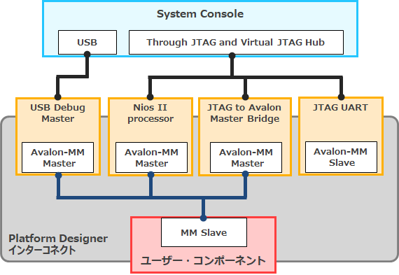
System Console คือ เครื่องมือที่ใช้ debug IP ที่ถูกสร้างโดย Qsys โดยใช้ JTAG เป็นตัวกลางในการสื่อสารระหว่าง System Console ⇔ FPGA ซึ่งความสามารถของ System Console จะสามารถ Access register ของ FPGA ด้วย Platform Designer (formerly Qsys) system แบบ Real-Time ถึงแม้จะไม่มี NIOS II บน FPGA ก็สามารถใช้ System Console ได้ พูดง่ายๆก็คือ Debug Hardware ผ่าน Avalon Bus
เนื้อหาของบทความด้านล่างนี้ จะเป็นการยกตัวอย่างการใช้งาน System Console อย่างง่าย เพื่อให้ผู้อ่านได้ทำความเข้าใจของหลักการทำงาน และ วิธีการใช้งาน
เครื่องมือที่ใช้ตามรายการด้านล่างนี้
- Quartus Prime Pro Edition / Standard Edition / Lite Edition
- FPGA Board ( FPGA ทุกตัวที่สามารถใช้งานได้บน Quartus Prime )
- Intel FPGA Download Cable ( USB-Blaster I or II )
ข้อกำหนดในการใช้งาน
การจะใช้งาน System Console ได้ จำเป็นจะต้องเชื่อมต่อสัญญาณแบบใดแบบหนึ่งตามรายการด้านล่างนี้
- JTAG to Avalon Master Bridge ( JTAG Master )
- Nios II Processor ( with JTAG Debug Module )
- USB Debug Master
- Avalon-ST ( Streaming ) JTAG Interface
- JTAG UART
- Ethernet Component
ตัวอย่างการใช้งาน System Console
เป็นการใช้ System Console ตรวจสอบสัญญาณ Clock, Reset และ Access register ของ DIP Switch, LED, On-Chip RAM เป็นต้น โดย Block Diagram แสดงดังภาพด้านล่างดังนี้
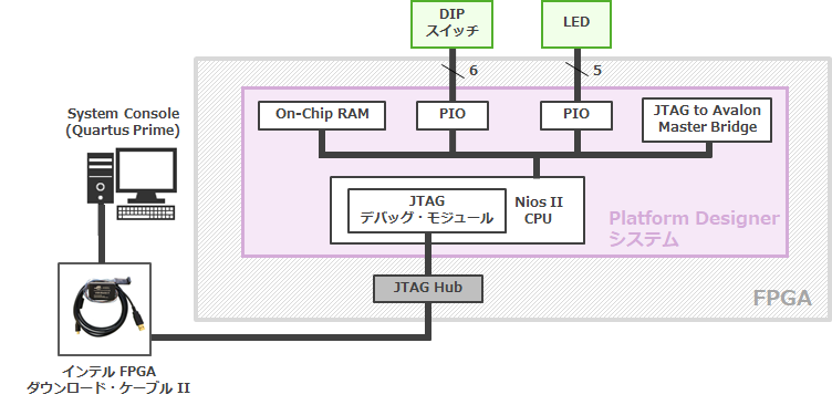
Photo by Macnica Japan
ต่อจากนี้ จะเป็นขั้นตอนการออกแบบโดยใช้ Quartus Prime Standard Edition โดยแบ่งออกเป็นหัวข้อย่อยได้ดังต่อไปนี้
- Platform Designer system
- Design Compilation
- Board Connection & FPGA Configuration
- System Console Starting
- Service Bus Setting
- Service Starting
- Debug Starting
- Service Closing
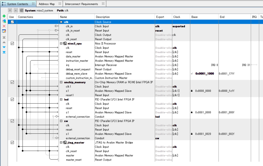
1.Platform Designer System
จากที่กล่าวข้างต้น การที่เราจะสามารถใช้งาน System Console ได้ จะต้องสร้างส่วนประกอบต่างๆให้ครบก่อน
ในหัวข้อนี้จะเป็นการเพิ่ม Component ต่างๆใน Platform Designer
- Nios II Processor ( with JTAG Debug Module )
- JTAG to Avalon Master Bridge ( JTAG Master )
- On-Chip Memory Intel FPGA IP ( Internal RAM )
- PIO Intel FPGA IP ( DIP Switch, LED )
note: ถ้าหากต้องการ Access register มีแต่ Nios II Process IP ตัวเดียวก็พอแล้ว แต่ในครั้งนี้เราต้องการใช้ JTAG Debug service จึงจำเป็นต้องเพิ่ม JTAG to Avalon Master Bridge เข้ามาด้วย
หลังจากที่เพิ่ม Component มาครบแล้ว ให้ทำการเชื่อมต่อ Component เข้าด้วยที่แทบ System Contents
โดยหลักการก็คือ Avalon Memory Mapped Master เป็นตัวสั่งงาน Avalon Memory Mapped Slave ให้ทำการเชื่อมต่อ Master เข้ากับ Slave ตามภาพด้านล่าง
note: ในตัวอย่างนี้ Master Service จะถูกดำเนินการโดย Nios II Avalon MM Master และ JTAG Debug Service จะถูกดำเนินการโดย JTAG to Avalon Master Bridge Avalon MM Master
เมื่อเชื่อมต่อเสร็จแล้ว ให้ทำการ save และ Generate HDL
2.Design Compilation
เมื่อ Generate HDL เสร็จแล้ว ให้นำไฟล์ที่ได้ไปรวมกับ FPGA Project Design แล้วทำการ Compile รวมอีกครั้ง
3.Board Connection & FPGA Configuration
- เชื่อมต่อ FPGA Board เข้ากับ Download Cable ( USB-Blaster I หรือ II ) จากนั้นให้ทำการจ่ายไฟเข้ากับบอร์ด
- เปิด Quartus Prime ไปที่ Programmer แล้วเลือก Hardware Setup เพื่อตั้งค่า Download Cable จากนั้น คลิ้กที่ Add file… แล้วเลือกไฟล์ .sof
- กดปุ่ม Start แล้วรอจน Configuration Progress ครบ 100% โดยไม่มี Error
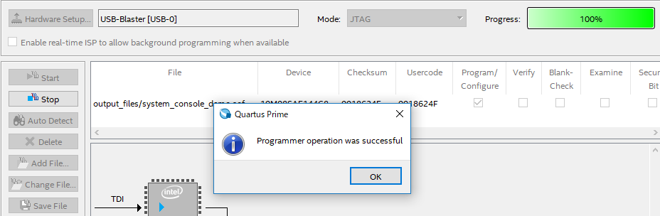
ปิดโปรแกรม Programmer
note : สำหรับ FPGA Configuration นั้น ไม่ได้ทำได้แค่ที่นี่เพียงอย่างเดียว ใน System Console ก็สามารถทำได้เช่นกัน ด้วย Command “device_download_sof” จะถูกกว่าในหัวข้อถัดไป
4.System Console Starting
- ทำการเปิด System Console
การเปิด System Console สามารถทำได้ด้วยกัน 3 วิธี สามารถเลือกวิธีใดวิธีหนึ่งได้ดังตัวเลือกด้านล่างนี้
A) Quartus Prime : Tools -> System Console
B) Platform Designer : Tools -> System Console
C) Nios II Command Shell : พิมพ์ system-console.exe - ทำการ Load Design โดยเลือกที่ File -> Load Design -> เลือก .sof < ถ้าหากโหลด .sof มาก่อนหน้าแล้ว สามารถข้ามขั้นตอนนี้ได้เลย >
- ไปที่แทบ devices จะเห็น devices folder ที่เป็นชื่อ FPGA ที่เราออกแบบ ให้ทำการคลิ้กขวา -> Program device -> เลือก .sof ไฟล์
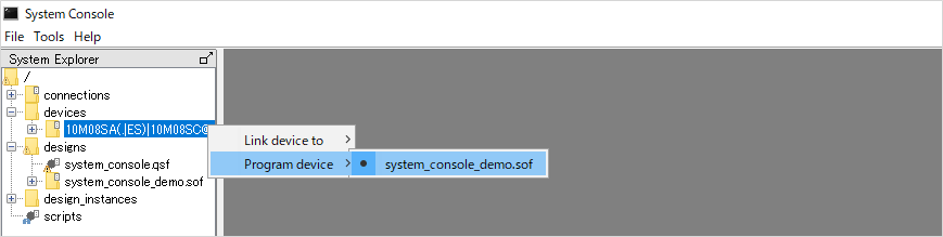
หรือจะ Program Device ด้วย Command line ด้านล่างนี้ก็ได้เช่นกัน
% get_service_paths device
% set dpath [lindex [get_service_paths device] 0]
% device_download_sof $dpath “sof file path”
5.Service Bus Setting
- ที่ Tcl Console ให้พิมพ์ Command Line นี้ ลงไป get_service_paths
สามารถตรวจสอบ Command List ได้โดยคำสั่ง get_service_types
สำหรับตัวอย่างนี้ เราต้องการ Access register ของ DIP Switch ( PIO ), LED ( PIO ), On-Chip RAM ให้ใช้ Master Service สามารถใช้ Command line ตามด้านล่างนี้
% get_service_paths master
เมื่อพิมพ์ Command Line แล้ว สำหรับตัวอย่างนี้ Avalon MM Master จะมีการแสดงผล 2 ตัว ( node0, node1 )
สามารถตรวจสอบได้ทั้ง Command Log และ บริเวณ System Explorer ตรง Folder -> FPGA part number -> link -> JTAG
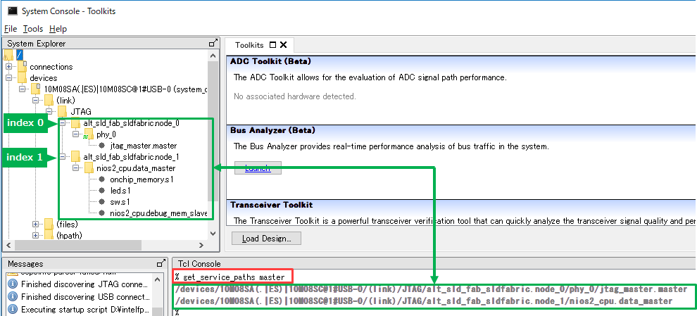
- สำหรับตัวอย่างนี้ เราต้องการอ่านและเขียน memory ของ slave ทุกตัว เราจึงเลือกตัวล่าง ( index 1 ) สามารถใช้ Command line ตามด้านล่างนี้
% set mpath [lindex [get_service_paths master] 1]
6.Service Starting
เราสามารถเริ่ม Service ที่กำหนดค่ามาแล้วข้างต้น ด้วย Command claim_service ได้เลย ตามด้านล่างนี้
% claim_service master $mpath “”
หลังจากนี้ เพื่อให้เวลาทำการ Debug สามารถทำได้ง่าย สามารถใช้ Command ด้านล่างนี้ได้เลย
% set master_path [claim_service master $mpath “”]
note : กรณีที่ใช้ Command line ด้านบนนี้ เป็นการรวม Command claim_service เข้าไปด้วยเลย ทำให้ไม่จำเป็นต้องใช้ claim_service master $mpath “”
7.Debug Starting
สำหรับการ Debug จะเริ่มหลังจากนี้เป็นต้นไป โดยให้ใช้ Command line ต่อไปนี้สำหรับ Debug ตามหัวข้อต่างๆ
- Clock & Reset signal Checking
Command ด้านล่างนี้ สำหรับตรวจสอบสัญญาณ Clock และ Reset
% set jdpath [lindex [get_service_paths jtag_debug] 0]
% jtag_debug_sample_clock $jdpath
% jtag_debug_sample_reset $jdpath
% jtag_debug_reset_system $jdpath
※jdpath lindex =0 ( ใช้ jtag_debug service ในการ debug )
jtag_debug_sample_clock : จะทำการ Loop Back สัญญาณ Clock
jtag_debug_sample_reset : จะทำการ Loop Back สัญญาณ Reset
jtag_debug_reset_system : จะทำการ Reset Component ทั้งหมด ที่ต่อกับ Avalon to JTAG Master
- DIP Switch On/Off Checking
Command ด้านล่างนี้ สำหรับอ่านค่า DIP Switch
% master_read_8 $master_path 0x10020 1
master_read_8 : ค่าของ Address ที่ต้องการอ่าน ครั้งละ 8 bit
0x10020 : DIP Switch ( PIO ) Address
1 : Size of Data
- LED On/Off Control
Command ด้านล่างนี้ สำหรับควบคุมการทำงานของ LED
% master_write_8 $master_path 0x10000 0x1F
% master_write_8 $master_path 0x10000 0x0
master_write_8 : ค่าของ Address ที่ต้องการอ่าน ครั้งละ 8 bit
0x10000 : LED ( PIO ) Address
0x1F、0X0 : ค่าที่เขียน (0x1F : All LED ON, 0x0 : All LED OFF )
- On-chip RAM Read/Write
Command ด้านล่างนี้ สำหรับอ่านและเขียน On-chip RAM
% master_read_32 $master_path 0x8000 32
master_read_32 : ค่าของ Address ที่ต้องการอ่าน ครั้งละ 32 bit
0x80000 : On-chip RAM Address
32 : Size of Data ( 32 bit )
% master_write_32 $master_path 0x8000 {0 1 2 3 4 5 6 7 8 9 10}
master_wrote_32 : ค่าของ Address ที่ต้องการเขียน ครั้งละ 32 bit
0x80000 : On-chip RAM Address
{0 1 2 3 4 5 6 7 8 9 10} : ค่าที่เขียน
Command ต่างๆ สามารถศึกษาเพิ่มเติมได้จาก Link ด้านล่างนี้
สำหรับ Standard Edition Lite Edition
Analyzing and Debugging Designs with System Console
「Intel Quartus Prime Standard Edition User Guide: Debug Tools」
สำหรับ Pro Edition
Analyzing and Debugging Designs with System Console
「Intel Quartus Prime Pro Edition User Guide: Debug Tools」
8. Service Closing
สำหรับการปิดการทำงานของ System Console จะ ปิดการทำงาน ตั้งแต่ หัวข้อที่ 6 ( Service Start ) สามารถใช้ Command ด้านล่างนี้ได้เลย
% close_service master $master_path
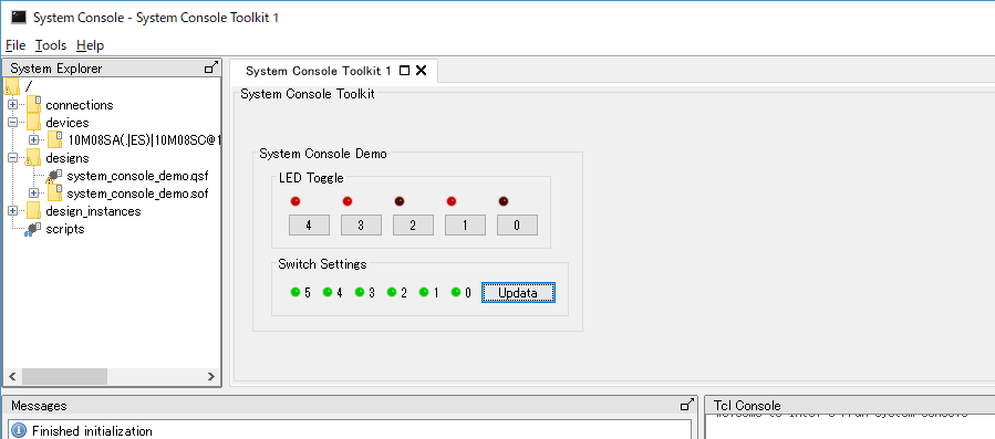
System console ยังสามารถนำข้อมูลที่ได้จากการ Command มาสร้างเป็นกราฟิกได้อีกด้วย โดยสร้างจาก Toolkit API ซึ่งผู้เขียนจะแนะนำวิธีใช้งานในบทความถัดไป
บทสรุป
การใช้งาน System Console เหมาะสำหรับการ Debug ฮาร์ดแวร์ทั้งระบบเบื้องต้น ก่อนจะส่งต่อให้นักพัฒนาเฟิร์มแวร์ เนื่องจากสามารถอ่านและเขียนข้อมูลของอุปกรณ์ทั้งหมด อีกทั้งยังสามารถตรวจสอบสถานะของสัญญาณนาฬิกาและสัญญาณรีเซ็ตได้อย่างรวดเร็วและง่ายดาย เพียงไม่กี่นาทีก็สามารถตรวจสอบได้แล้ว
ก็จบไปสำหรับบทความนี้นะครับ หวังว่าจะได้ประโยชน์อะไรบ้างจากบทความนี้ไม่มากก็น้อยนะครับ ยังไงถ้าถูกใจกับบทความนี้ก็ฝากกด like ด้วยนะครับ หรือจะส่งความคิดเห็น, คำแนะนำ, ข้อเสนอแนะและคำถามที่สงสัยมาเพิ่มเติมก็ได้นะครับ
โดยทาง NDRS มีความรู้จากผู้เชี่ยวชาญมาคอยแบ่งบันเรื่อยๆ หากกำลังมองหาผู้เชี่ยวชาญเพื่อมาช่วยแก้ปัญหาให้กับผลิตภัณฑ์อิเล็กทรอนิกส์ สามารถติดต่อมาทางอีเมล์ ndrs@ndrsolution.com ได้ครับ
เนื้อหาทั้งหมดอ้างอิงจาก https://www.macnica.co.jp/business/semiconductor/articles/intel/134097